A double-sided copper substrate PCB is a double-sided copper based printed circuit board, which includes circuits on the top and bottom layers. It is a commonly used printed circuit board. A double-sided copper substrate PCB can be wired and welded on both sides, with a metal copper core in the middle and an insulation layer between the circuit and the copper core. Both sides can be connected, greatly reducing the difficulty of wiring and therefore widely used. Both sides of a double-sided copper substrate PCB are wired, but in order to use the wires on both sides, there must be appropriate circuit connections between the two sides, and the "bridge" between the circuits is called a guide hole. A guide hole is a small hole filled or coated with metal on a PCB board that can connect wires on both sides. We call it a true double-sided copper substrate PCB when designing a double-sided circuit board with guide holes. It can also be designed as a double-sided circuit without connection, which is the same as a regular single-sided circuit board but can achieve the same installation efficiency as a double-sided circuit board. We call it a fake double-sided copper substrate PCB. Due to the fact that the area of a double-sided panel is twice that of a single panel, the double panel solves the problem of staggered wiring in a single panel and can be connected to the other side through holes, making it more suitable for circuits more complex than a single panel.
What we are introducing now is a fake double-sided copper substrate PCB, also known as a fake double-sided thermoelectric separation copper substrate PCB and a 2-layer copper circuit board PCB.
1. False double-sided thermoelectric separation copper substrate PCB
Introduction to false double-sided thermoelectric separation copper substrate PCB product:
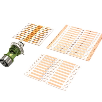
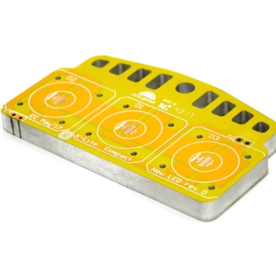
False double-sided thermoelectric separation copper substrate PCB (double-sided thermoelectric separation copper substrate PCB) is generally used for automotive high and low beam integrated lamp panels or products with heat dissipation needs. High power heat dissipation is achieved through two large protrusions on the upper and lower sides, and the external heat dissipation aluminum parts are connected to the position of the double-sided protrusions for heat dissipation; At the same time, the upper and lower currents of the double-sided thermoelectric separation copper substrate PCB are connected through vias, and only one side of the welding electrode is needed to control the lighting of the upper and lower sides of the lamp beads, the protrusion for heat dissipation, and the circuit for conduction. This is called double-sided thermoelectric separation. The product has advantages such as large heat dissipation, low power consumption, stable performance, and easy installation.
2. Schematic diagram of the PCB structure layer of the fake double-sided thermoelectric separation copper substrate:
.jpg)
Pseudo double-sided thermoelectric separation copper substrate pcb, "heat" refers to the thermal conductive pad (PAD) on the LED copper substrate pcb, and "electricity" refers to the electrodes on the LED copper substrate, both of which are isolated by insulating materials. The function of a thermal conductive pad (PAD) is to conduct heat, and the function of the electrode is to conduct electricity. This double-sided structure can achieve LED heat dissipation design and provide product stability. The structure of the double-sided thermoelectric separation PCB is shown in the figure:
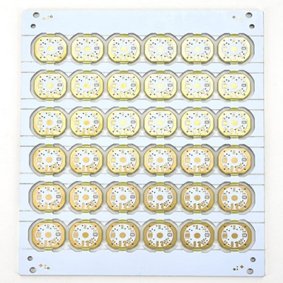
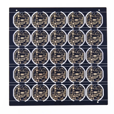
3. Schematic diagram of the front and back sides of the fake double-sided thermoelectric separation copper substrate PCB product:
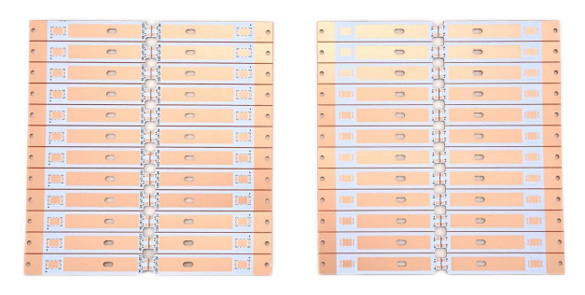
4. False double-sided thermoelectric separation copper substrate PCB product type:
True double-sided copper core PCB (via conduction) False double-sided copper PCB (without via) 2-layer copper substrate PCB 4-layer copper substrate PCB
5. Instructions for the production and production process of fake double-sided thermoelectric separation copper substrate PCB products:
a) Substrate: Red copper (C1100)
b) Thickness: 0.6-5.0MM
C) Number of layers: 1, 2, 3, 4 layers
d) Copper foil thickness: 1/2/3/4 OZ
e) Solder resistance color: white/black/matte black/red/green/blue/matte green
f) Character color: white/black/orange/red/blue
g) Forming method: CNC gongs, CNC V-cutting, mold forming, laser cutting and milling
h) Surface treatment process: Lead sprayed tin, lead-free sprayed tin, chemical gold precipitation (gold thickness 0.5U "~3.0U"), chemical nickel palladium gold OSP
i) Inspection and testing: AOI, high-speed flying needle, electronic testing, voltage withstand test
g) Delivery time: 6-8 days.
6. Pseudo double-sided thermoelectric separation copper substrate PCB product application scenarios:
Flashlights, industrial mining lights, automotive LED headlights, UV lights, stage projection lights, 5G communication, wall washing lights, LED street lights, mechanical equipment, and various precision and high demand heat dissipation lighting instruments
7. Advantages of fake double-sided thermoelectric separation copper substrate PCB products:
Long service life, efficient heat dissipation, stable performance, and wide application range
8.FAQ
Q1. Are you a PCB manufacturer? Do you have a factory?
Answer: We are a professional manufacturer of printed circuit boards for over 12 years. We have factories and machines, and you can see pictures of our factories.
Q2. Can I obtain PCB samples for free? Can you deliver the goods free of charge?
Answer: Yes, we can provide you with a free PCB sample after discussing and confirming all the detailed information. But we do not provide free delivery services. If you purchase a large quantity of products, we will give you some discounts.
Q3. Do you do OEM?
Answer: Yes. We are a manufacturer of printed circuit boards, and we have factories and dedicated automation equipment for the entire process of PCB and PCBA, providing precise inspection and shipment. We provide one-stop procurement services for PCB and PCBA.
Q4. Can you produce a PCB with thermal conductive pads in direct contact with the substrate and electrodes on another layer?
Answer: Yes, we can produce PCBs with thermal conductive pads in direct contact with the substrate, which we call thermoelectric separation copper substrates. You can send Gerber information to our email address [email protected] Confirm.
Q5. Can copper core PCBs be produced with copper holes?
Answer: Yes, there are copper holes on both sides of the copper core PCB to conduct and connect the circuit. We call it a true double-sided copper substrate PCB, and we have many years of manufacturing experience in metal core printed circuit boards.


